Webcam project
How we built an IoT webcam from scratch with a ATSAM4S and a WiFi chip.


This was the project that started it all. This was the final project of the class Engineering System Design I. In this class, we were taught how to design and produce a webcam from scratch, from the programming, to the PCB and CAD design of the case.
Design
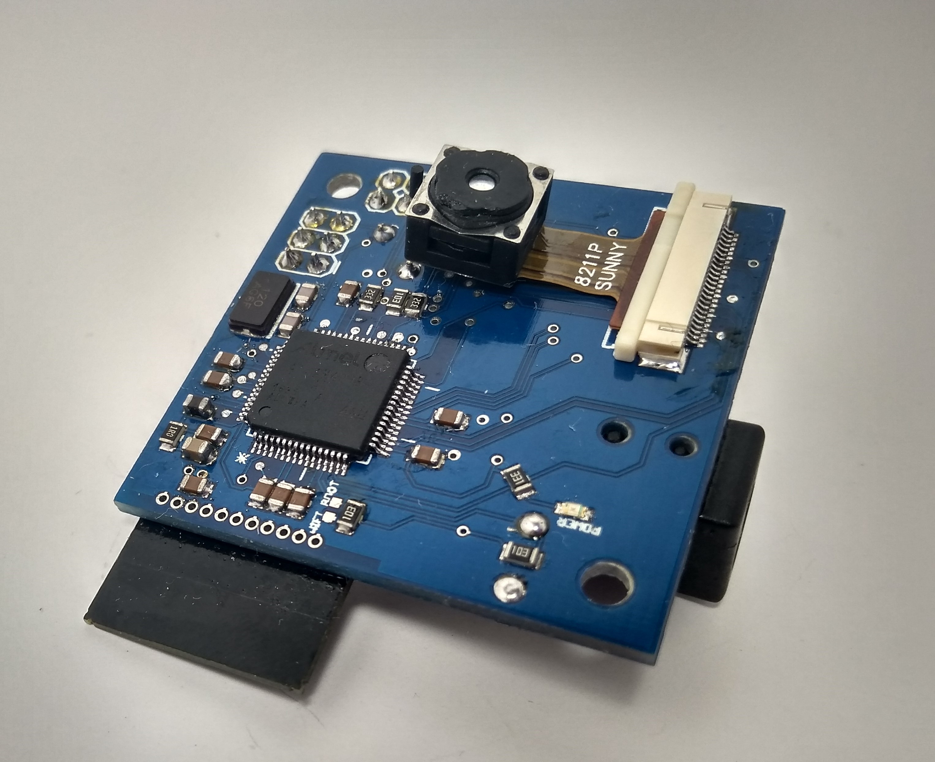
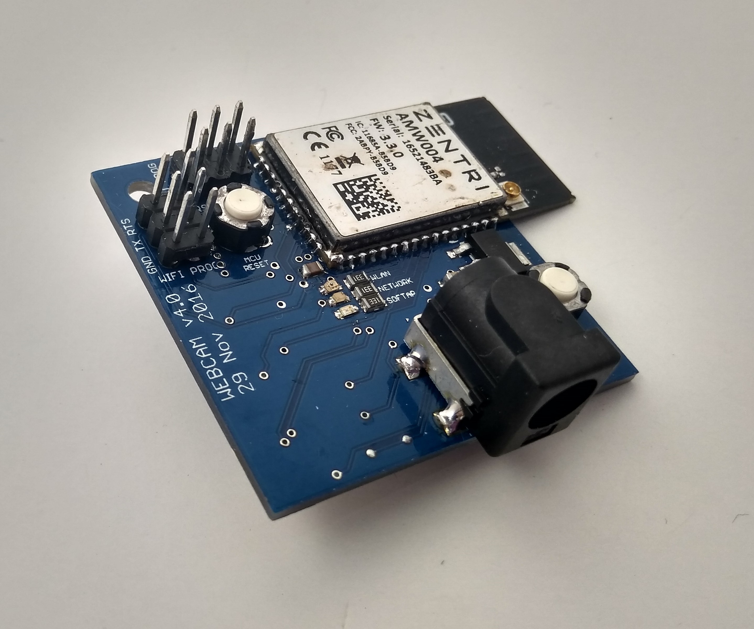
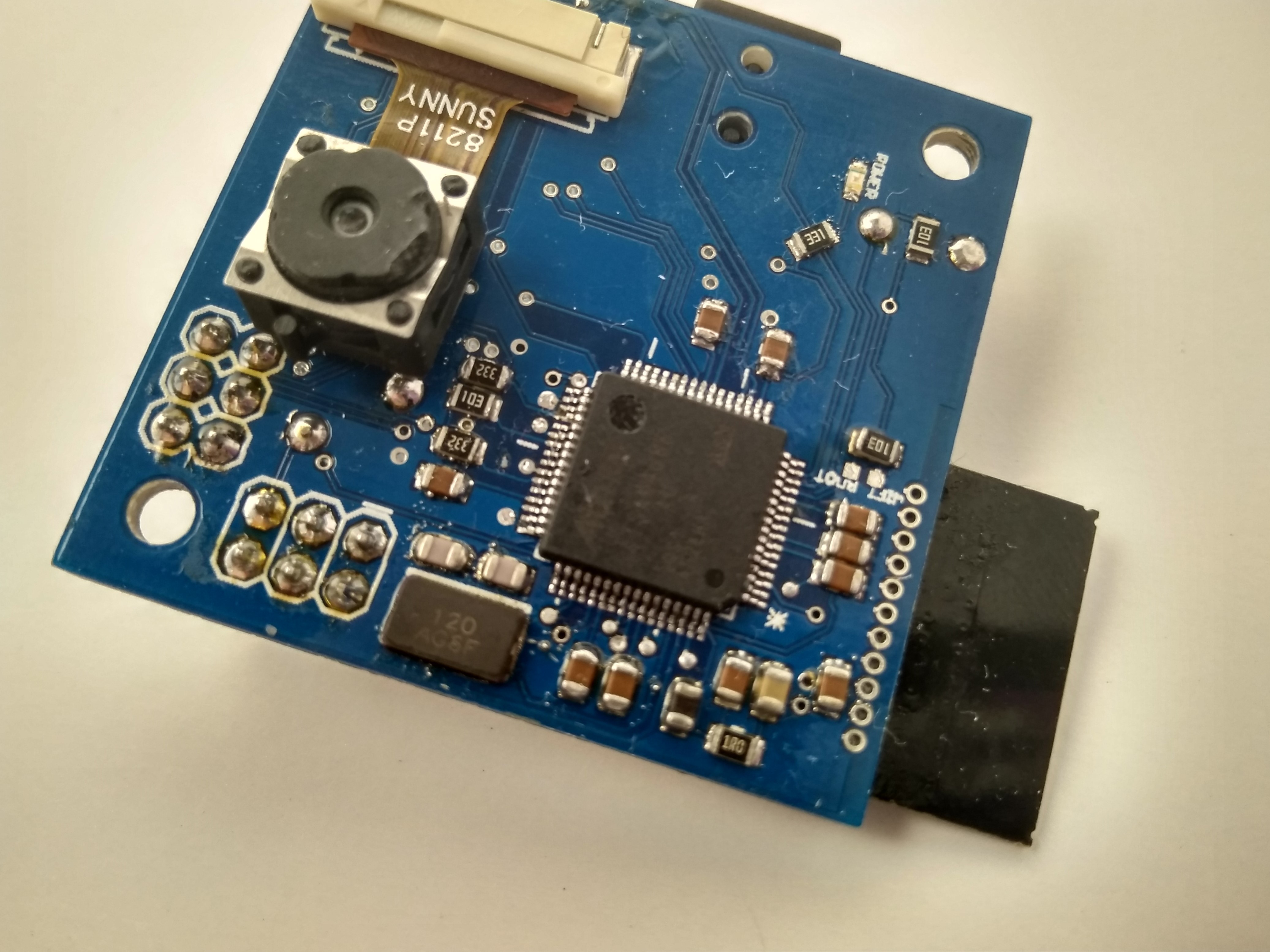
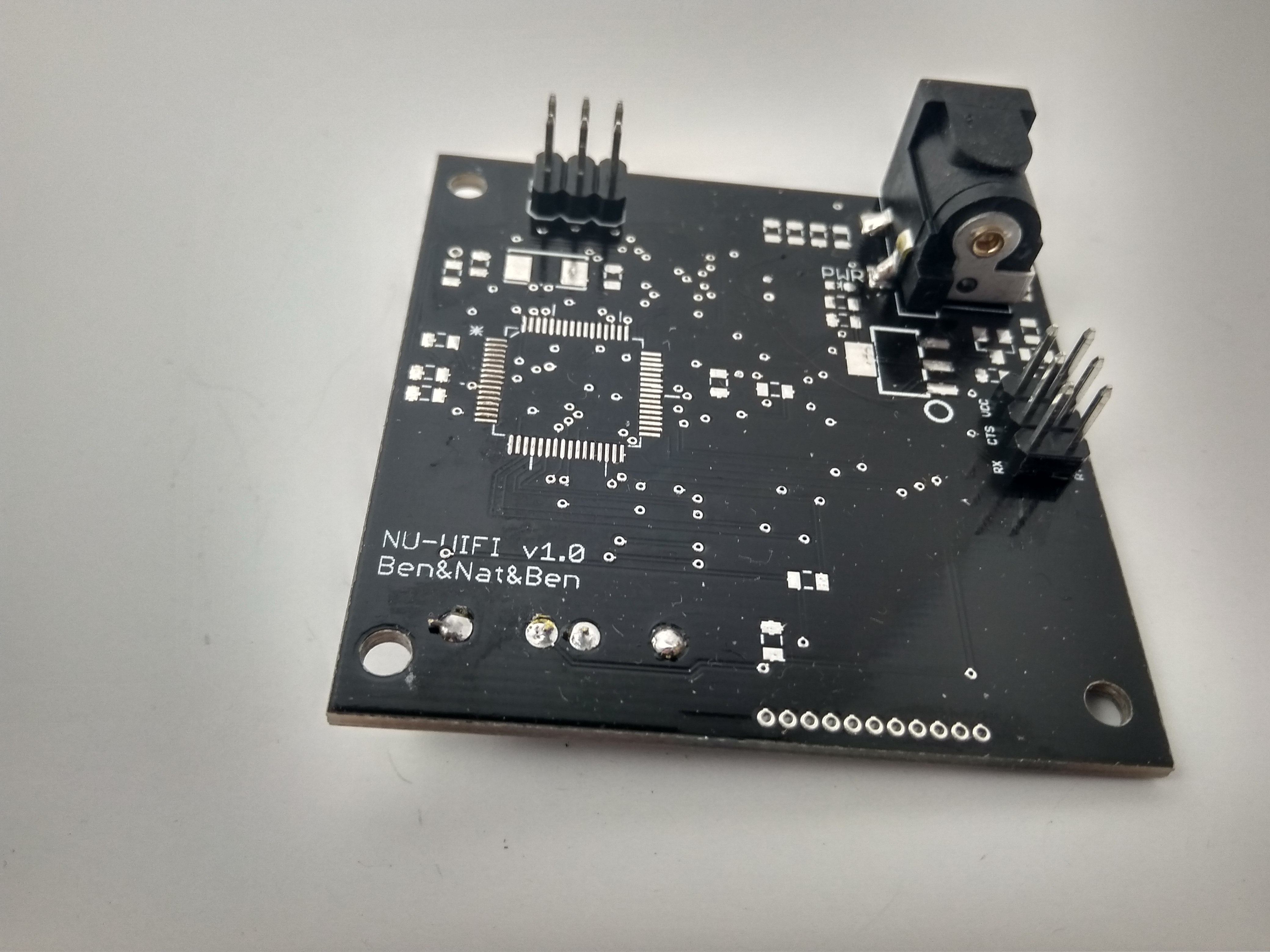
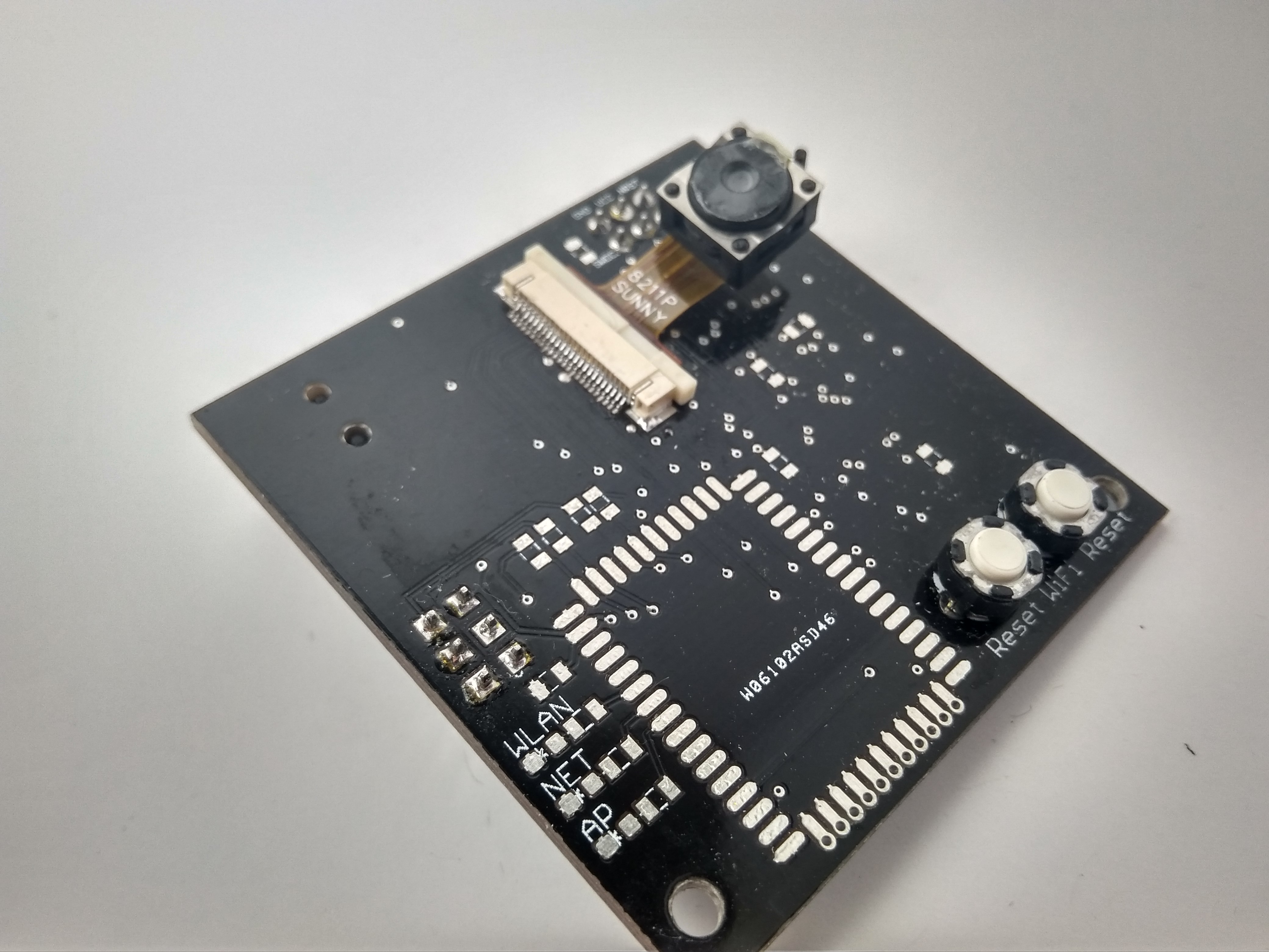
This webcam is driven by a ATSAM4S8B chip. It processes the incoming data from the OV2640 webcam and stores it to memory before streaming it bit-by-bit to the Zentri WiFi chip on the reverse side. The Zentri chip is programmed to connect to the wireless network as well as host a website to display the images. Without optimization, our design was able to display images at a rate of about 3 frames a second.
The power comes from a 3.5mm jack and it is stepped down from 12V to 3.3V for both the SAM4S and the Zentri chip. A powered jack was used because the system draws quite a bit of power in use. Two buttons reset the MCU as well as set up the WiFi for the system. There are indicator LEDs to indicate the WLAN, Network, and the SoftTap status of the Zentri chip, as well as one on the reverse side to indicate power is flowing to the MCU.
Process
We first had to learn how to solder SMD components, and we were given a practice board with practice chips.
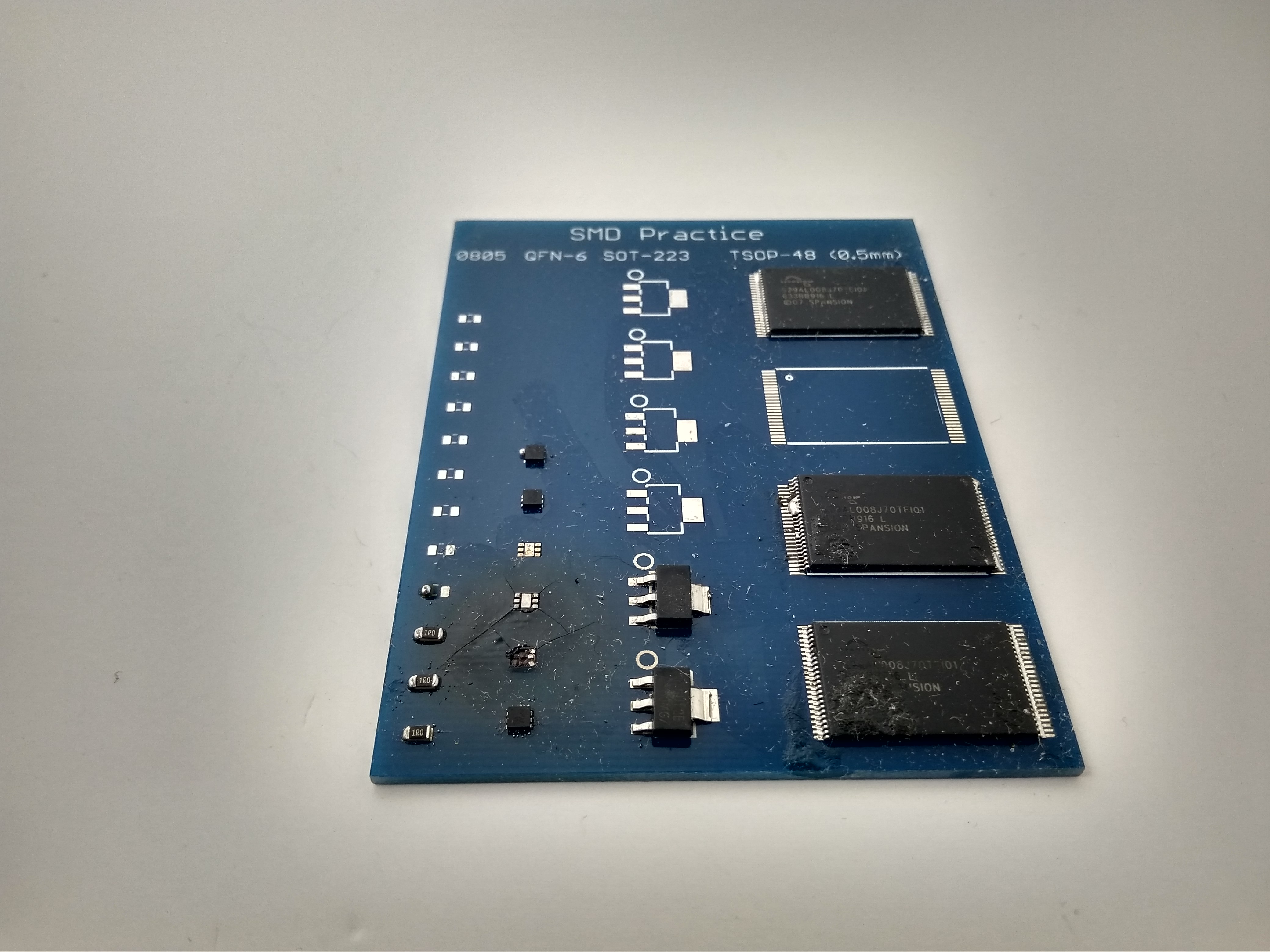
That burnt part there is what happens when you increase the temperature of the hot air gun by 50$^\circ$C to remove a part faster. It is good to practice before doing the real thing.
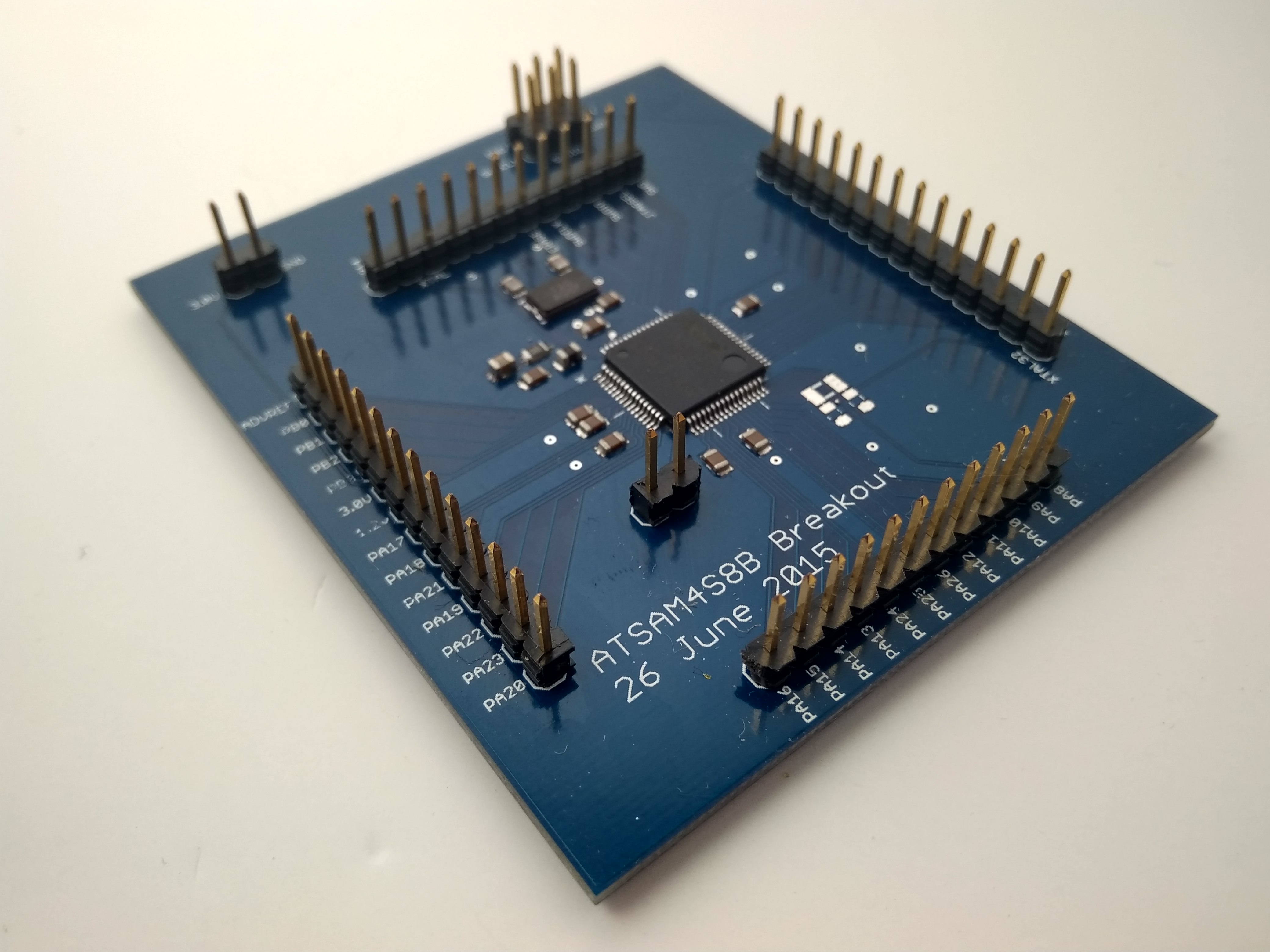
Once we mastered soldering, we had to break out all the pins on the ATSAM4S for prototyping. To that end we were given a minimalist breakout board with only the bare components necessary for the chip to work. We programmed the chip using an Atmel ICE debugger over the SWD interface in Atmel Studio.
The camera and the WiFi chip both had their breakout boards, and the WiFi chip was used to power the MCU as it had a 3.3V output regulator and was programmed over USB. All the boards were connected using a breadboard and it was a huge tangle.
There were some mistakes made when developing and designing this board. The earliest one was where I swapped a 0 ohm resistor with a capacitor to disastrous results. I didn't see any smoke, but the 3.3V line was 1.2V, which was very bad, and I could not figure out why for the longest time, checking power and ground leads until I went over each component and found the offending part.
Because the chip was castellated, when I tried to desolder it from a non-working board, I ended up taking off the top cover as well as bending the antenna a little because of how long I was heating it for without trying to remove the existing solder.
On another board, as we were soldering in the headers for the MCU programming pins, because we heated it for so long, we managed to pull off a pad and it could no longer be used. Since this was the last part, we had to desolder everything and resolder it on a new board.
One of the connections was wrong on our original board and even though we tried to rewire it by using a white wire, the connection just wasn't reliable enough for us to ensure that it was working, so we had to abandon our PCB design and instead, relied on the instructor's board.
Conclusion
This project was not easy. Even with all the groundwork laid out for us, and with almost two months worth of time, we were still basically unsuccessful in producing our own attempt. However, we did learn a lot and personally, a lot of what I learnt has gone forward as other successful projects.